
Practical FPGA: How to start (Altera)
 In this series of articles I will talk about how to start working with FPGA (Field Programmable Gate Array). Even basic knowledge of FPGA/CPLD architecture opens new understandings about hardware development possibilities especially if you are targeting real-time processing which might be complicated or impossible on modern CPU/MCU running operating systems.
Development board
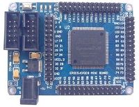
Some time ago I purchased cheap Altera EP2C5T144 development board from eBay it was collecting dust and waiting to serve it’s purpose. I will be using it for my tests today.

EP2C5T144 mini demo board
USB Blaster for flashing compiled files was already included in the package. Whole kit was in a range of 30-40$ including shipping. There are multiple sellers on eBay, Aliexpress and other online shops – this board is pretty popular. Though Xilinx Spartan family is also pretty popular, I will talking about Altera this time.

USB Blaster
Installing tools
Altera provides free limited tools to work with it’s devices. Which is in most cases more than enough. It’s called Quartus II Web Edition. At the moment newest version is 15.1, but support for older Cyclone II devices were discontinued in 13.1. Latest usable version is 13.0 SP1. Minor disadvantage – in order to download you will need to create account on Altera web page. There not much you can do wrong installing this software and I will not describe how to do this. In general press Next, Next, Next…
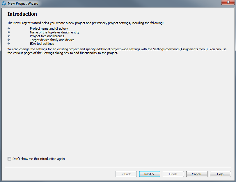
First project
Now I will step through simple project creation. Provide project location, name and device to be used.
New…
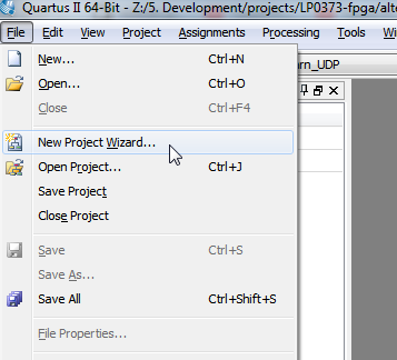
Chose New Project Wizard…
Next >

Provide project path and name

Skip this step. Next >

Select Cyclone II Family and EP2C5T144 device

Leave as it is. Next >

Project summary

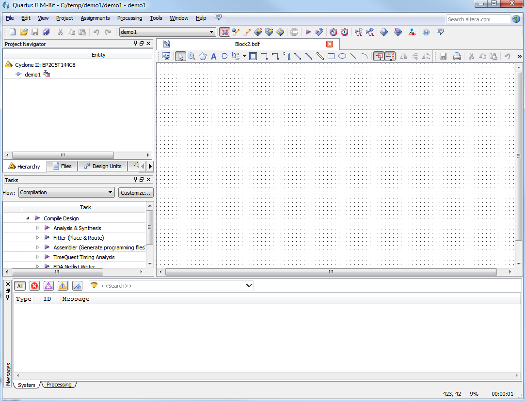
Fresh project window
Configure pins
In order to make software know what pin properties and connected hardware you have to define it.

Click on Pin Planner

FPGA device footprint opens
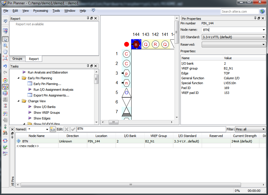
Zoom, double click on desired pin and enter it’s name.
This development board has following devices attached:
- PIN_17 – 50MHZ
- PIN_3 – LED1
- PIN_7 – LED2
- PIN_9 – LED3
- PIN_144 – BTN
Don’t need to save, pin configuration is updated once you enter information.
Simplest possible project “1_button_led”
This project will connect input and output pins. Button with LED and once you press button LED state will be changed.

Add new file to project

It will be Block Diagram/Schematic File
Fresh Diagram/Schematic window
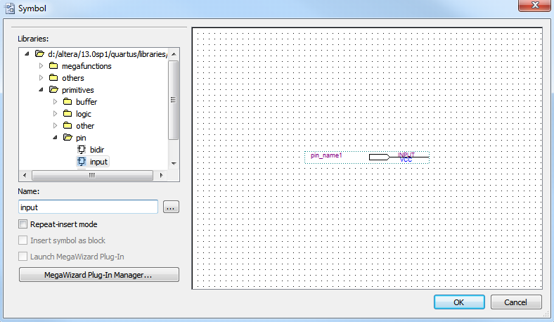
Double-click and enter “input” in Name field. You can also navigate to pin / input section in tree menu.
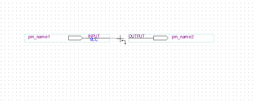
Do the same just this time place output pin. Connect these ports by dragging a line between them.

Double-click in ports and rename input to BTN, output to LED1

CTRL+S – saves your project
Compile/Synthesize
Congratulations! First FPGA project is complete. Now let’s synthesize the hardware.

Click on button Start Compilation
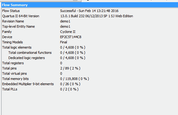
It will take a while and provide summary on job completion
Congratulations oce again. You have succeeded to compile first simplest possible FPGA project. Next step will be uploading compiled project to FPGA itself.