
Practical FPGA: How to flash (Altera)
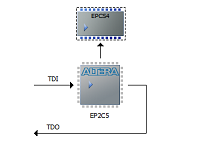 Altera EP2C5T144 FLGA has no internal configuration flash memory and can be programmed two ways. One is to configure temporary – good method for testing and debugging. Another – over the same interface flash soldered flash chip. This is tricky and hardly documented step. In this post I am providing working recipe how to program flash device over USB Blaster over FPGA.
Programmer
I mentioned in previous post that I will be using Bus Blaster programmer which was bundled together with FPGA development board. This has to be best option for the beginner.
Run on hardware
When project is compiled next logical step is to run it on real hardware. Of course simulating and testing performance is also useful step, but this time we will skip directly to hardware testing. I will be using the same project – button controls LED.

Click on button Programmer
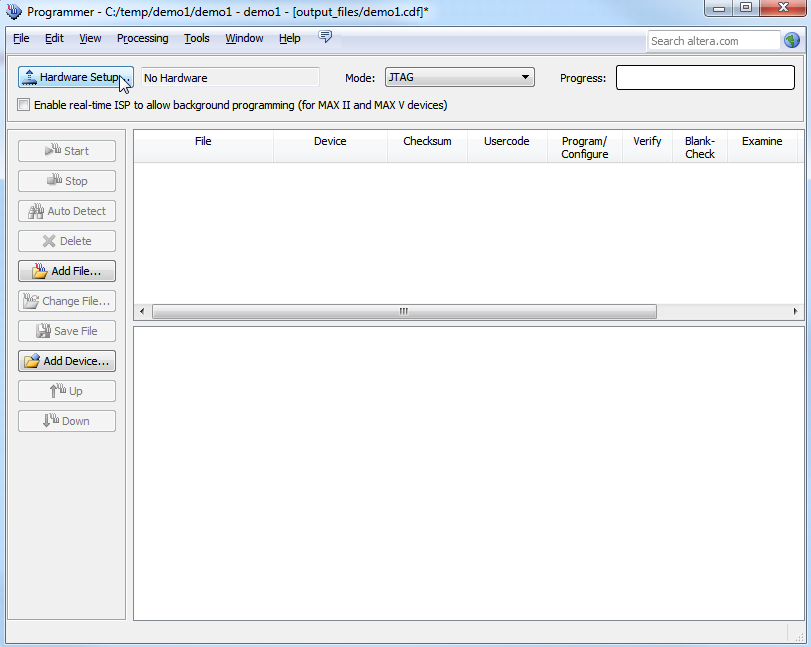
Setup programmer hadrware

Select installed USB Blaster
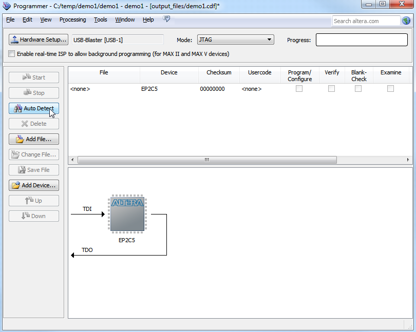
Click Auto Detect and hopefully connected FPGA will be detected

Chose demo1.sof file to be programmed

Tick Program/Configure check box and Start button will become activated

In a few seconds it status should become 100% (Successful)
Results
By completing this step you will get demo project working on FPGA hardware. This step writes binary file to FPGA itself and after rebooting device it will be blank. Following recipe will provide you information how to write firmware to flash.
Write to flash
Writing compiled file to installed flash device is not trivial. It involves couple of file conversions with included tools and correct sequence pressing right buttons. This kind of complexity is caused of flexibility of Altera tools. It is possible to flash several FPGA’s or flash devices in one programming procedure. So, follow provided steps to program your designed logic into your board.
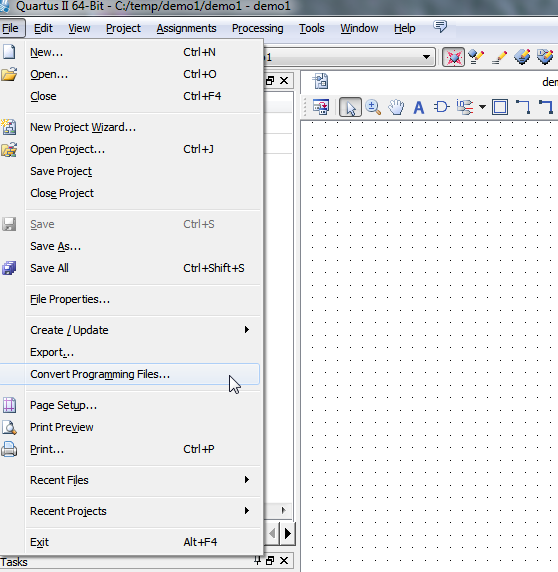
Convert file format
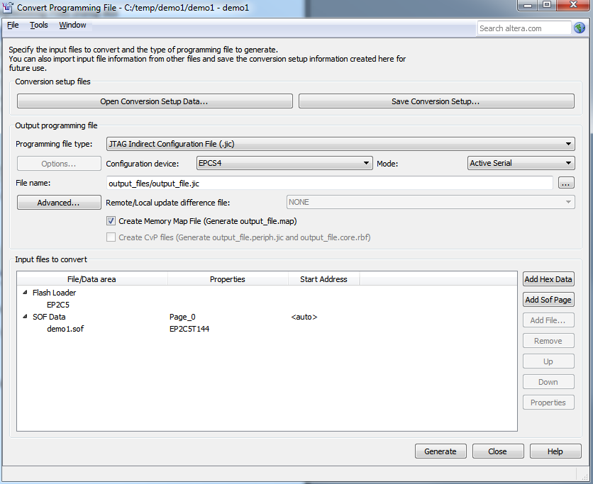
Fill information like provided screenshot. Programming device: JTAG Indirect Configuration File (.jic), Configuration device: EPCS4, Flash loader -> Add Device…, SOF data -> Add file
Now open programmer window

Create JAM. JBC, SVF or ISC File…
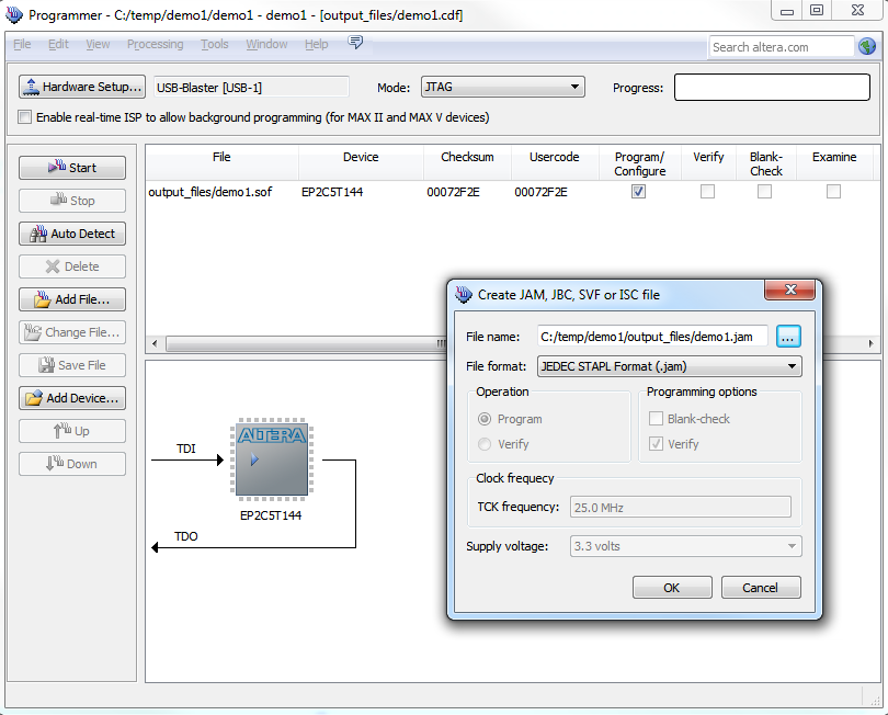
Leave as it is and click OK
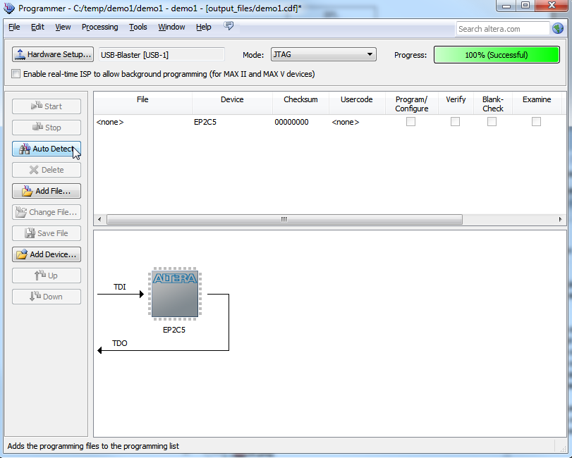
Remove existing file and click Auto Detect
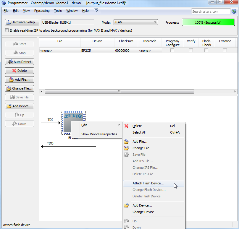
Attach flash device…

Chose installed flash device
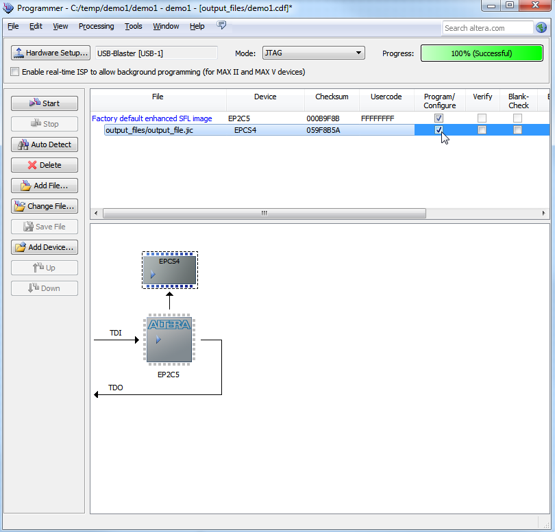
Add generated .jic file to flash device and tick Program/Configure check box

Click Start and few in a moments you should have programmed demo board. After power cycle it will still be running your project